MEMS & Semiconductors
MEMS foundry, CCD foundry, high-reliability chipsets
The Number 1
Indepedent Pure-Play MEMS Foundry in the World.
Products
Our semiconductor services are unusual and exceptional. From consumer electronics to automobiles , optical networking equipment to biomedical “lab on chip” devices, MEMS (micro electromechanical systems) are everywhere, and Teledyne offers the #1 independent pure play MEMS foundry capability in the world. We also offer advanced system-on-chip development and packaging services for high-reliability multi-chip modules for extreme environments.
MEMS Foundry Services

High Reliability Components
CCD Foundry Services
Fabrication Facilities and Capabilities
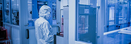
Our MEMS and microfabrication capabilities offer our customers an ideal solution to reach their markets quickly. From design to prototyping on 150mm wafers, through to high volume 200 mm production, Teledyne customers have access to a truly unmatched toolbox of proven and patented process modules and techniques.
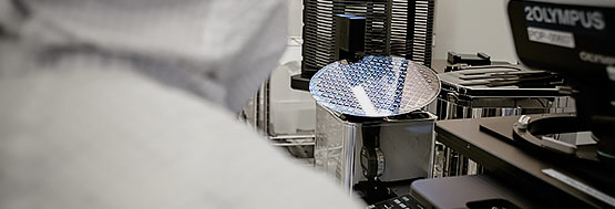
Our foundries boast more than 60,000 square feet / 5,600 m2 of clean rooms that operate 24/7 and deliver over 100,000 wafers per year in both 150 mm and 200 mm formats. Our state-of-the-art processes and industry-leading quality systems allow us to exceed our customer requirements.
Applications
Optical and Microbolometers
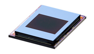
With our expertise in optical technologies, we enable our customers to implement smaller, faster, function-rich and cost-effective optical systems. If your project involves precise optical alignment, a laser optical bench, an optical filter structure or the use of a complex mirror, Teledyne has a solution.
Learn about silicon optical bench, mirror arrays, actuation, spatial light valves and micromirrors.
Our novel wafer-level packaging (WLP) approach to microbolometer manufacturing in an optimized MEMS infrastructure gives us the ability to dramatically alter the traditional price-performance tradeoff.
Acoustic and RF MEMS
Radio Frequency MEMS
Radio Frequency or RF MEMS describes a wide range of disparate devices and technologies. Teledyne has been manufacturing MEMS resonators and bulk acoustic wave (BAW) filters for several years.
Acoustic MEMS
MEMS technology enables multiple sensors to be put into devices where it would not be feasible to place conventional technology. MEMS can enable IoT voice-activated controllers and devices, like wearables, automobile sensors, and smart speakers.
Inertial Sensors
Inertial sensors are used to measure aspects of physical movement like thrust, velocity, angle and direction, and are widely used in consumer applications like smart phones, game consoles, automotive air bag systems and GPS displays.
Inertial sensors are used in oil and gas exploration, geological survey equipment, medical devices and aerospace. Regardless of application, MEMS-based inertial sensors require complex and precise etching techniques to create fine geometries that are consistent across the wafer.
Our experience in inertial sensors, including multi-axis and multi-function devices includes milestones in miniaturization as well as some of the world’s best vacuum and hermeticity capabilities.
Environmental Sensors
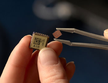
Environmental sensor applications include gas and Volatile Organic Compound (VOCs) monitoring, temperature, and pressure monitoring. Environmental sensors have wide-ranging applications in healthcare, automotive, defense and industrial environments.
Pressure sensors are among the most widely used environmental sensors. MEMS silicon wafer manufacturing allows for cost reduction and scalability to large volumes. MEMS-based gas sensors allow dramatic size reduction, a significant power consumption reduction, and the ability to increase functionality and selectivity using multisensory arrays on a single chip.
Our pressure sensor manufacturing experience includes piezoresistive and capacitive sensors used for a wide variety of automotive and industrial applications.
BioMEMS
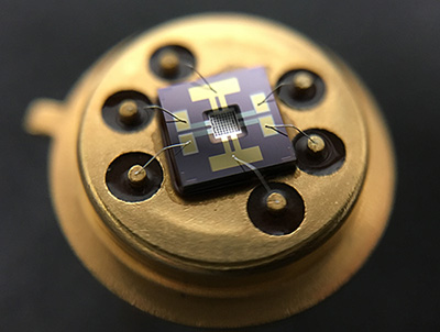
Success in the health sector depends on design reliability, speed of testing new technologies, and speed to market. MEMS and microtechnology advances can accelerate design and lower development costs and are driving the revolution in biological measurements and point-of-care diagnostics. Emerging innovations in medical analysis and non-invasive treatment call for unique application requirements such as multi-sensor connectivity and low-power consumption.
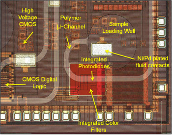
Our MEMS and microfabrication capabilities for biotechnology include silicon and glass microfluidics, CMOS post processing, thin film bioassay substrates, CMUT arrays for medical imaging, as well as other biomedical devices.
Our strength is in our ability to reach the high levels of integration needed in stand alone point-of-care products. Our advanced packaging options and proven high-volume manufacturing capability make us your ideal foundry partner for the bio-MEMS designs that will change the future.
Microfluidics
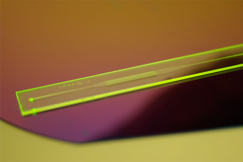
Microfluidic chips and end-use devices for applications such as lab-on-a-chip range widely, from designs for single sample injection to complex designs for multiple samples/diluent addition, microfluidic mixing, and microfluidic separation.
Applications of microfluidics include genomic analysis, proteomic separation and analysis, flow cytometry, threat detection, water analysis and cell analysis.

